
LongServing Technology Introduces the World’s First 2 nm Photonic Quantum Chip Material "X Photon" and Redefines the Future of Semiconductors and AI Computing
LongServing Technology Co. Ltd. of Taipei, Taiwan has announced that they have made a significant breakthrough which could change the future of semiconductor and photonics and artificial intelligence forever. The company's founder and CEO Dr. Ko Cheng Fang created a photonic quantum material called "X-Photon" that is the world's first at a 2-nanometer wavelength X-ray shortwave. An important breakthrough for the industry, as well as the next generation of ultra-fast, energy-efficient photonic computing technology.
For the first time, researchers can now produce and emit X-ray (photons) at the same wavelength of 2-nanometers. This will allow researchers to develop chips that can operate using light as opposed to electrons, which can solve many of the physical barriers which have been limiting progress in the semiconductor field for more than 40 years.
The Development and Breakthrough of New Electronic Chip Materials
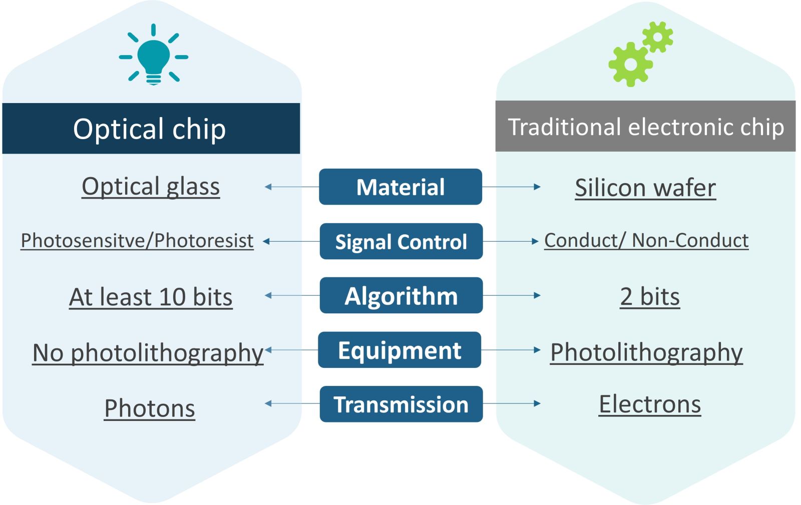
As we are beginning to reach the limitations of Moore's Law and the physical limitations of electronic systems are holding us back, the development of a new type of chip is occurring. Currently, our chips are designed using copper interconnects that cannot become any smaller than approximately 14 nanometers (nm) in width. As the size of the conductor is reduced, a number of different physical barriers exist for the flow of electrons. These barriers are excessive heat generation, quantum tunneling, increased resistance, and delays in the transmission of signals. These barriers have made it extremely difficult to make significant advances in the energy efficiency and performance of chips.
Electronics have been replaced by photonics for many research groups as the basis for a new type of electronic chip. However, currently available photonic materials can only support wavelengths much larger than what is necessary to create photonic pathways on today’s chip. Currently, silicon photonics supports wavelengths of between 1310 nm and 1550 nm, and quantum dots operate at wavelengths generally falling within the range of 300 nm to 700 nm. The dimensions required to create photonic pathways inside a chip cannot be scaled down from these wavelengths; therefore, there are no photonic pathways that can replace copper wiring in high density chips.
For the first time in history, the X Photon technology removes this barrier. The fact that X Photon uses a 2 nm wavelength allows for the creation of photonic pathways that will fit on chip level dimensions. This technology allows for the use of actual light to perform computations in a semiconductor architecture.
A New Era of Computing with New Materials
The X Photonic is a new class of material that has not been possible before, and it offers three significant advances in research that make this material one of the most important scientific breakthroughs of the last ten years.
1. Photons that Behave at True 2 Nanometers
This material allows for stable transmission of photons at a wavelength that is smaller than any current electronic conductor based on electronic components to date. With this innovation, optical signals can be transmitted through the chip with precision down to the nanoscale.
2. The Replacement of Copper Interconnects
For the first time, a material can facilitate photonic communication at a wavelength smaller than the size of a copper wire, allowing for extreme speed, low energy and extremely high-speed data transfer within microchips.
3. A Basis for Future Quantum Photonic Computing
The 2 nm wavelength permits quantum-scale interactions to occur on a chip level. The result is a real-world basis for photonic quantum enhancement and for next-generation AI acceleration.
These advances signify the transition from the electronic age into the photonic era; in the future, instead of generating heat and resistance as electrons do, light will carry information within future chips with almost no loss of energy.
Scientifically Verified and Technologically Transformative
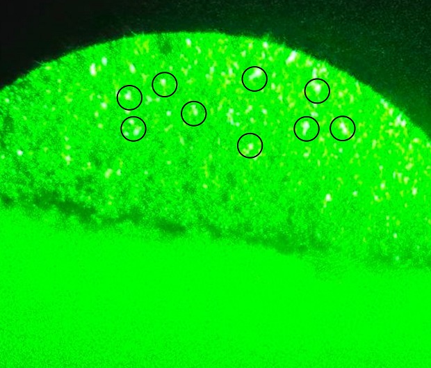
Based on scientific observations using advanced technology such as Raman Spectroscopy, X-Ray Diffraction and High-Resolution Electron Microscopy, X Photon has been shown to have unique photonic properties which are different from any other known natural structure. When excited with a laser, the material produces a distinct array of energetic wavelengths in white light that confirms the 2nm photonic emission.
The nanoscale pathways in the lattice structure of X Photon cannot be adequately described by electron microscopy techniques due to the extremely small size and the way that photons interact with the lattice structure. As a result, X Photon represents a new material classification.
About
Dr. Ko Cheng Fang is a pioneer in the field of photonic materials, semiconductor physics and the development of quantum chips. Dr. Fang has spent many years researching new forms of matter that can support ultra-short wavelengths of light for practical computation. His research with X Photon has placed him at the forefront of the next wave of globally advancing technology.
LongServing Technology Co., Ltd is a science-based company located in Taipei, Taiwan. This company focuses on developing advanced semiconductor materials and conducting research into photonic computation and next-generation chip technology. The company's goal is to develop revolutionary technologies that push the envelope of physics and make computing capabilities unimaginable.